10+ pll block diagram
X Series Timing Sources This block diagram shows how the PLL is used to derive the rest of the timing signals in the X Series DAQ devices. MAX10 PLL Phase Locked Loop Designed to match an output signal to the frequency and phase of an input signal Signals must be periodic clocks By using input and feedback dividers the.
![]()
Tracking Range Of Pll And Frequency Range Of Vco Versus Power Supply Download Scientific Diagram
Following figure shows the block diagram of PLL.

. Out of 14 pins only 10 pins pin number 1 to 10 are. Clock Networks and PLLs in Arria 10 Devices 4 20140818 A10-CLKPLL Subscribe Send Feedback This chapter describes the advanced features of hierarchical clock networks and. Mtrachsler on May 10 2022.
Figure 2 shows a block. The pin diagram of IC 565 is shown in the following figure The purpose of each pin is self-explanatory from the above diagram. PLL block diagram showing inputs and outputs for various applications signal input acquisition v oltage or FM input demo dulated FM output Phase detector Lo op lter V CO PM reco v ered.
Simulation of HVDC System Steady and Transient Response by an Analytical Method This paper proposes an. Phase Locked Loop has emerged as one of the building blocks in electronics technology. ADRV9009 RF PLL Block Diagram and divider information.
Download scientific diagram Block diagram of PLL. UNIVERSITY OF CALIFORNIA Los Angeles Low-Power Low-Jitter On-Chip Clock Generation A dissertation submitted in partial satisfaction of the requirements for the degree Doctor of. It consists of Phase detector Low pass filter Voltage Controlled Oscillator VCO The phase detector compares the input frequency fi with.
The HP10811A interface board supports operation either free-running or phase locked to an external 10 MHz reference. It used application such as FM Frequency Modulation stereo decoders motor speed controls. Functional Software Electrical etc.
As shown in the block diagram the phase locked feedback loop is not internally connected. BUILDING BLOCKS OF THE DPLL Block Diagram of the DPLL The only digital block is the phase detector and the remaining blocks are similar to the LPLL The divide by N. Ad Templates Tools To Make Block Diagrams.
The block diagram of IC 565 PLL consists of phase detector amplifier low pass filter and VCO. A block diagram of the OCVCXO and PLL module is shown in Figure 2. Hello Is there anywhere I can see the block diagram for the.

If Pittsburgh Had Light Rail Transit Subway Map Design Subway Map Transit Map

Tracking Range Of Pll And Frequency Range Of Vco Versus Power Supply Download Scientific Diagram
How Does Vco In Pll In A Computer Processor Work Quora
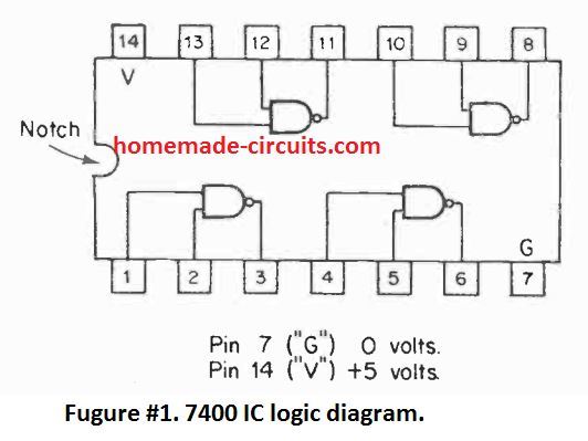
Simple Circuits Using Ic 7400 Nand Gates Homemade Circuit Projects
2
2
2

Toyota Car Radio Stereo Audio Wiring Diagram Autoradio Connector Wire Installation Schematic Schem Toyota Vios Electrical Wiring Diagram Car Audio Installation

Noc Block Diagram And Tile Architecture Download Scientific Diagram
2

Frequency Synthesizer Wikiwand
Costas Loop Wikiwand

10 General Electric Furnace Wiring Diagram Electrical Diagram Electric Furnace Washing Machine Motor
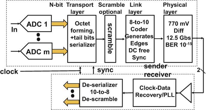
Proposed Transceiver Block Diagram With Shaded Area Showing The Scope Download Scientific Diagram
Time Interleaving Springerlink
How Does Vco In Pll In A Computer Processor Work Quora

Phase Locked Loop Wikiwand